Skip to Content
MilliporeSigma
All Photos(1)

Documents

799009

Sigma-Aldrich

Monolayer graphene film

1 in x 1 in on copper foil, avg. no. of layers, 1

Synonym(s):

Graphene/Cu

Sign Into View Organizational & Contract Pricing


About This Item

UNSPSC Code:
12352103
NACRES:
NA.23

Quality Level

description

Coverage: >95%
FET Electron Mobility on Al2O3: 2;000 cm2/V·s
FET Electron Mobility on SiO2/Si (expected): 4; 000 cm2/V·s
Grain size: Up to 10 μm
Number of graphene layers: 1
Transparency: >97%

form

film

feature

avg. no. of layers 1

resistance

350 Ω/sq

L × W × thickness

1 in. × 1 in. × (theoretical) 0.245 nm, monolayer graphene film
1 in. × 1 in. × 18 μm, copper foil substrate

color

transparent

Looking for similar products? Visit Product Comparison Guide

Related Categories

General description

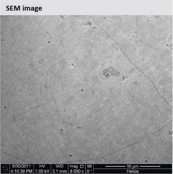
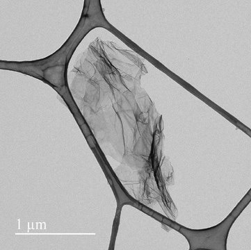
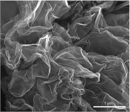
Graphene is a unique one atom thick, two dimensional allotrope of carbon. Among all the synthesis techniques, chemical vapor deposition of graphene on copper foil is the most promising route for the large scale production of good quality graphene. Catalytic decomposition of hydrocarbons over copper foil renders monolayer graphene. Graphene deposits as a continuous polycrystalline sheet of individual graphene grains joined at grain boundaries. The epitaxial relationship between graphene and copper foil has been reported. Large uniform graphene domains may be accountable to the large grain size growth which results because of the low carbon solubility of copper and close melting point of copper and graphene growth temperatures.
Growth Method: CVD synthesis
Transfer Method: Clean transfer method
Quality Control: Optical Microscopy & Raman checked

Application

Graphene may be extensively incorporated in several applications, such as; nanoelectronics, fuel cells, solar cell, photovoltaic devices, in biosensing, optical biosensors, MEMS, NEMS, field effect transistors (FETs), chemical sensors, nanocarriers in biosensing assays.

Storage Class

11 - Combustible Solids

wgk_germany

WGK 3

flash_point_f

Not applicable

flash_point_c

Not applicable


Certificates of Analysis (COA)

Search for Certificates of Analysis (COA) by entering the products Lot/Batch Number. Lot and Batch Numbers can be found on a product’s label following the words ‘Lot’ or ‘Batch’.

Already Own This Product?

Find documentation for the products that you have recently purchased in the Document Library.

Visit the Document Library

Customers Also Viewed

Slide 1 of 1

1 of 1

Graphene powder, electrical conductivity >103 S/m, avg. no. of layers, < 3

Sigma-Aldrich

900561

Graphene

Jianing Chen et al.
Nature, 487(7405), 77-81 (2012-06-23)
The ability to manipulate optical fields and the energy flow of light is central to modern information and communication technologies, as well as quantum information processing schemes. However, because photons do not possess charge, a way of controlling them efficiently
Experimental observation of a suspended single layer graphene film on Cu foil grown via chemical vapor deposition method
Won-Hwa Park, Myunghee Jung, Jin-San Moon, et al.
Physica Status Solidi (A): Applied Research, 250(9), 1874-1877 (2013)
Xuesong Li et al.
Science (New York, N.Y.), 324(5932), 1312-1314 (2009-05-09)
Graphene has been attracting great interest because of its distinctive band structure and physical properties. Today, graphene is limited to small sizes because it is produced mostly by exfoliating graphite. We grew large-area graphene films of the order of centimeters
Weak mismatch epitaxy and structural feedback in graphene growth on copper foil.
Wilson NR, et al.
Nano Research, 6(2), 99-112 null
Functionalized CVD monolayer graphene for label-free impedimetric biosensing
Eissa S, et al.
Nano Research, 8(5), 1698-1709 null

Articles

Professor Gogotsi and Dr. Shuck introduce MXenes: a promising family of two-dimensional materials with a unique combination of high conductivity, hydrophilicity, and extensive tunability.

Advanced technologies for energy conversion and storage are widely sought after for their potential to improve consumer and electronic device performance as well as for the prospect of reducing the societal and environmental impact of energy generation.

Advances in scalable synthesis and processing of two-dimensional materials

See All

Our team of scientists has experience in all areas of research including Life Science, Material Science, Chemical Synthesis, Chromatography, Analytical and many others.

Contact Technical Service