FIPMS176
Back-gated OFET Substrate
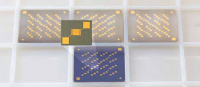
n-doped silicon wafer with 230 nm SiO2 gate-insulator, chips (diced)
About This Item
Recommended Products
form
chips (diameter 200 mm)
chips (diced)
packaging
pack of 1 (wafer of 112 diced chips)
Related Categories
General description
Layer structure:
- Gate: n-doped silicon (doping at wafer surface: n~3x10¹⁷/ cm3)
- Gate oxide: 230 nm ± 10 nm SiO2 (thermal oxidation)
- Drain/source:none
- Protection: resist AR PC 5000/3.1 (soluble in AZ-Thinner or acetone)
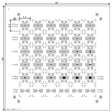
- Layout: bare oxide but diced
- Chip size: 15 x 15 mm2
- No. of chips: 112 per wafer
Application
These back-gated organic filed-effect transistor (OFET) substrates were fabricated inside the cleanroom, and source and drain electrodes can be deposited either prior or after the deposition of an organic semiconductor material, giving versatility for the choice of source/drain materials and satisfy different preferred device architectures.
When an organic semiconductor layer is deposited on such a substrate, the bulk Si acts as gate electrode and controls the channel current between the post-deposited source and drain electrodes on the top. A suitably doped Si-SiO2 interface in CMOS quality guarantees a reproducible gate contact.
Packaging
Preparation Note
To guarantee a complete cleaning of the wafer / chip surface from resist residuals, please rinse by acetone and then dry the material immediately by nitrogen (compressed air).
Recommendation for material characterization:
If gate currents appear during the characterization of the field effect transistors, considerable variations could occur at the extraction of the carrier mobility. Therefore it is necessary to check the leakage currents over the reverse side (over the chip edges) of the OFET-substrates.
Storage and Stability
Legal Information
Certificates of Analysis (COA)
Search for Certificates of Analysis (COA) by entering the products Lot/Batch Number. Lot and Batch Numbers can be found on a product’s label following the words ‘Lot’ or ‘Batch’.
Already Own This Product?
Find documentation for the products that you have recently purchased in the Document Library.
Articles
Professor Tokito and Professor Takeda share their new materials, device architecture design principles, and performance optimization protocols for printed and solution-processed, low-cost, highly flexible, organic electronic devices.
Our team of scientists has experience in all areas of research including Life Science, Material Science, Chemical Synthesis, Chromatography, Analytical and many others.
Contact Technical Service


