798177
Suspended monolayer graphene on TEM grid substrate (Quantifoil gold)
About This Item
Recommended Products
form
solid
Quality Level
resistance
170 Ω/sq
diam. × thickness
2 mm × (theoretical) 0.345 nm , monolayer graphene film
size × distance between discs × diam.
2 μm × 4 μm × 3 mm, gold coated TEM grid
Related Categories
General description
Graphene Film Properties
Growth Method: CVD synthesis
Transfer Method: Clean transfer method
Size: 2 mm (TEM grid diameter)
Appearance (Color): Transparent
Transparency: >97%
Coverage: >95%
Number of graphene layers: single layer
Thickness of the lazy carbon is about 12 nm.
FET Electron Mobility on Al2O3: 2; 000 cm2/Vs
FET Electron Mobility on SiO2/Si (expected): 4; 000 cm2/Vs
Sheet Resistance: 170 Ohms/sq.
Grain size: up to 10 micrometer
Substrate TEM grid
Type: QUANTIFOIL(registered) R 2/4
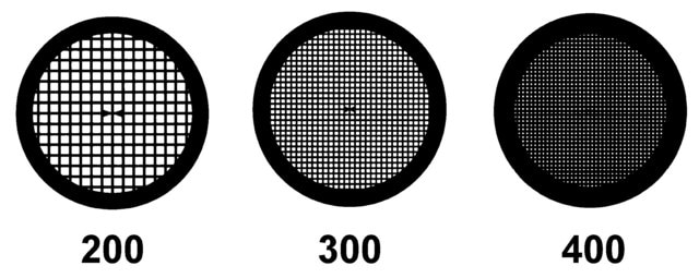
Hole Size: 2 micrometers(Au grid is 300 mesh)
Space between holes: 4 micrometers
Diameter: 3 mm
Coating: Au coated
Application
Storage Class
11 - Combustible Solids
wgk_germany
WGK 3
flash_point_f
Not applicable
flash_point_c
Not applicable
Certificates of Analysis (COA)
Search for Certificates of Analysis (COA) by entering the products Lot/Batch Number. Lot and Batch Numbers can be found on a product’s label following the words ‘Lot’ or ‘Batch’.
Already Own This Product?
Find documentation for the products that you have recently purchased in the Document Library.
Customers Also Viewed
Articles
Graphene is a one-atomic-layer thick two-dimensional material made of carbon atoms arranged in a honeycomb structure. Its fascinating electrical, optical, and mechanical properties ignited enormous interdisciplinary interest from the physics, chemistry, and materials science fields.
Advanced technologies for energy conversion and storage are widely sought after for their potential to improve consumer and electronic device performance as well as for the prospect of reducing the societal and environmental impact of energy generation.
Advances in scalable synthesis and processing of two-dimensional materials
Our team of scientists has experience in all areas of research including Life Science, Material Science, Chemical Synthesis, Chromatography, Analytical and many others.
Contact Technical Service
